


Electronic Circuit Board — Repair & Rework Guide
A practical, step-by-step repair reference for electronics technicians, engineers, and advanced hobbyists. Written for a UK audience with reference to applicable international standards.
Contents
1.Introduction
Once a fault has been identified on an Electronic Circuit Board (ECB) using systematic diagnostic techniques, the next stage is competent, controlled repair. ECB repair demands patience, the correct tools, sound technique, and a thorough understanding of the materials involved. Poor rework can cause additional damage, introduce new faults, or compromise the long-term reliability of the repaired assembly.
This guide covers the full range of ECB repair and rework techniques applicable to both through-hole and surface-mount (SMD) assemblies, including soldering, desoldering, component replacement, track and pad repair, via repair, and the application and removal of conformal coatings. The procedures are consistent with IPC-7711/7721 (Rework, Modification and Repair of Electronic Assemblies), the internationally recognised standard for ECB repair.
2.Safety & Regulatory Requirements
2.1Regulatory Framework (UK)
All ECB repair and rework carried out in a UK professional or commercial environment is subject to:
- Health and Safety at Work etc. Act 1974 (HSWA) — the primary duty on employers and employees to ensure safe working practices.
- Electricity at Work Regulations 1989 (EAWRs) — all soldering and component work must be carried out with the board de-energised.
- COSHH 2002 — governs solder, flux, solvents, IPA and conformal coatings; a written COSHH assessment must be in place for all substances used.
- PUWER 1998 — governs the suitability and safe use of soldering stations, hot air rework tools and ancillary equipment.
- WEEE Regulations 2013 — governs disposal of removed components, waste solder and contaminated materials.
2.2ESD Precautions
All ECB repair work must be carried out under full ESD precautions as specified in BS EN 61340-5-1 (UK/EU) or ANSI/ESD S20.20 (international):
- Wear a tested and calibrated ESD wrist strap connected to a common bonding point throughout all handling and rework.
- Work on a grounded ESD mat connected to the same common bonding point.
- Store removed components in ESD-safe packaging immediately.
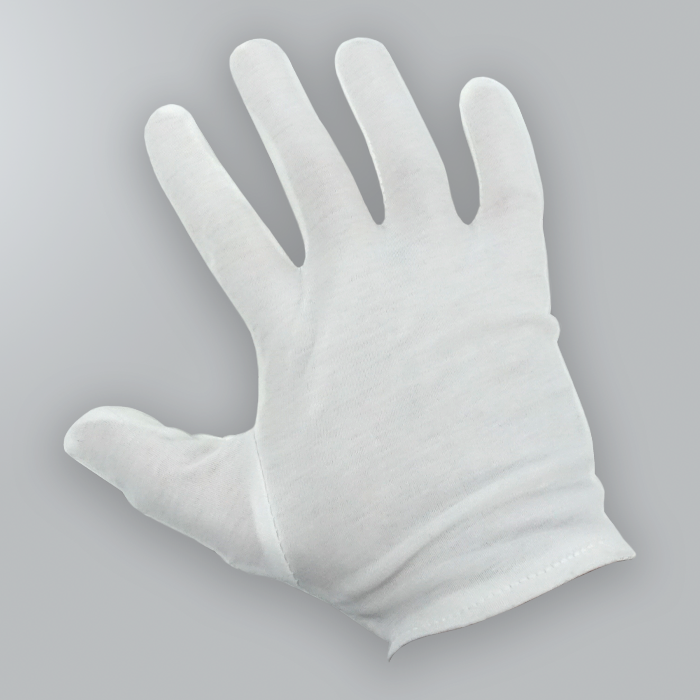
- Take replacement components from ESD-safe packaging and handle them without touching leads or pins directly.
2.3Ventilation & Fume Extraction
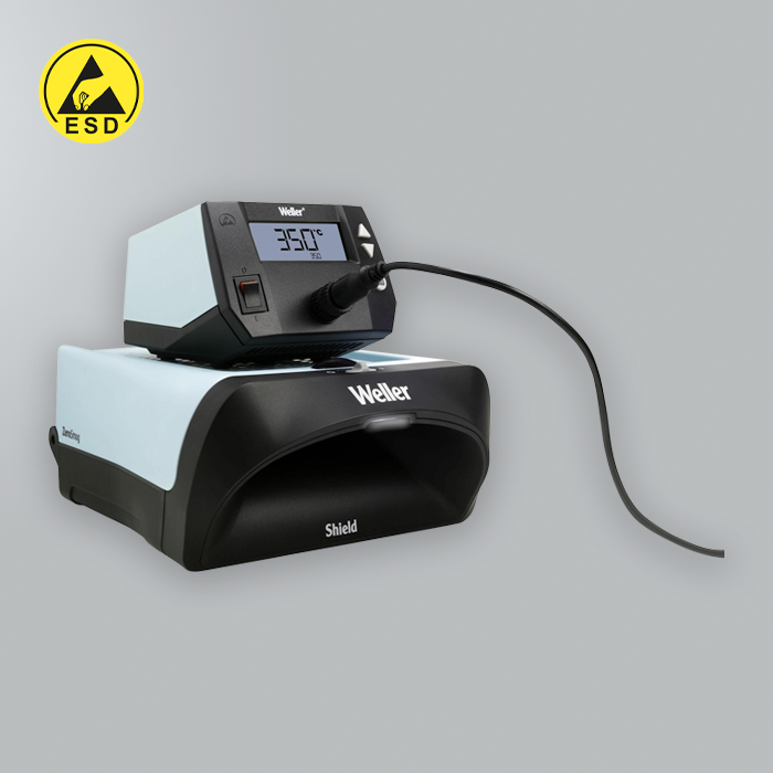
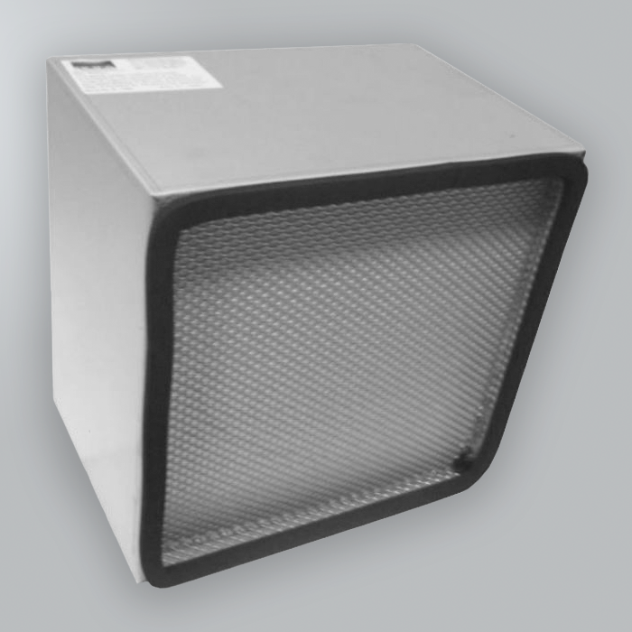
- A fume extraction unit with a correctly rated filter must be positioned within 150 mm of the soldering point.
- Filters must be replaced in accordance with the manufacturer's schedule and the COSHH assessment.
- Lead-free solder fume is not harmless: SAC305 alloys produce tin and silver particulate which are respiratory hazards.
- Lead-based solder (Sn63/Pb37) presents both fume and surface-contamination hazards: wash hands thoroughly and do not eat, drink or touch your face during or after soldering without washing first.
3.Tools, Materials & Workspace
3.1Essential Equipment
The following equipment is required for competent ECB repair work. Improvised or unsuitable tools are a leading cause of repair-induced damage and must not be used.
| Equipment | Specification | Notes |
|---|---|---|
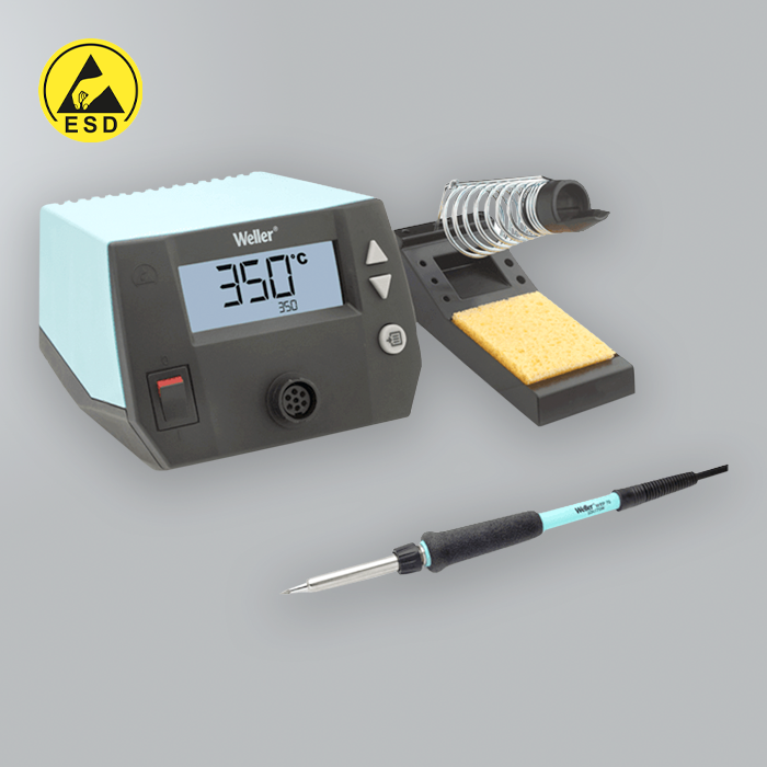
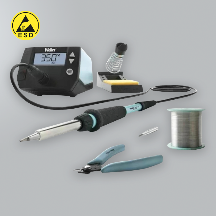
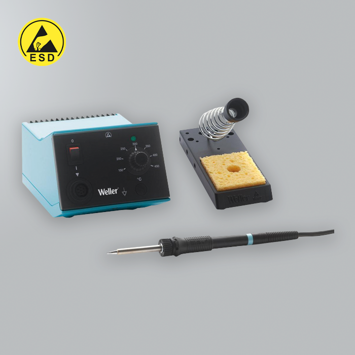
| Soldering station | Temperature-controlled, 48–80 W, 200–480 °C | Never use an uncontrolled mains iron on PCBs |
| Hot air rework station | Adjustable temperature and airflow; interchangeable nozzles | Essential for SMD removal; match nozzle to package size |
| Solder | SAC305 (lead-free) or Sn63/Pb37 (leaded), 0.5–1.0 mm flux-cored | Match alloy to the original assembly where possible |
| Flux | No-clean or RMA rosin flux, pen or liquid | Water-soluble flux must be fully cleaned after use |
| Desoldering tools | Solder sucker and desoldering braid (1.5–3.5 mm) | Pre-flux the wick before use for better absorption |
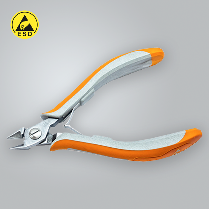
| ESD tweezers | Fine-tip, anti-static, stainless steel | Keep tips clean and undamaged |
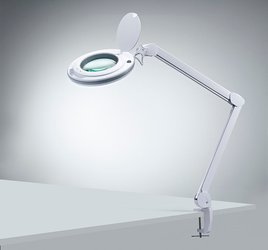
| Magnification | Stereo microscope (10–40×) or illuminated loupe (10× min.) | Stereo microscope essential for fine-pitch SMD work |
| Cleaning materials | IPA 99%, ESD-safe brushes, lint-free swabs | Do not use household cleaning products on PCBs |
| PCB holder / third hand | Adjustable, ESD-safe PCB vice or holder | Free hands are essential for precise rework |

3.2Soldering Iron Tip Selection & Maintenance
The iron tip is the most critical variable in soldering quality. An incorrectly selected, worn or poorly maintained tip causes the majority of rework defects.
- Chisel tips (2–4 mm) — most versatile; through-hole joints, drag soldering, general SMD work.
- Conical / pencil tips (0.5–1 mm) — fine-pitch SMD, targeted heat application.
- Knife / hoof tips — drag soldering of fine-pitch QFP and SOIC packages.
- Maintenance — tin the tip with fresh solder before and after each use; clean on a damp sponge or brass wool between joints; replace when the plating is visibly pitted, black or porous.
3.3Workspace Setup
- Set up on a clean, clear ESD mat connected to a common bonding point.
- Position the fume extraction unit within 150 mm of the work area.
- Ensure adequate lighting and magnification appropriate to the component pitch.
- Have all tools and materials within reach before starting, to minimise movement of the PCB.
- Secure the PCB in a holder or vice — never solder a board resting loose on the bench.
- Keep a lint-free cloth and IPA to hand for immediate tip cleaning and flux removal.