Electronic Circuit Board — Fault Finding & Diagnosis Guide
A systematic, step-by-step reference for electronics technicians, engineers, and advanced hobbyists. Written for a UK audience with reference to applicable international standards.
Contents
- Introduction
- Safety Precautions
- Test Equipment
- Systematic Fault Finding Process
- Information Gathering & Pre-Inspection
- Visual Inspection
- Power Supply Rail Verification
- Component-Level Testing
- Signal & Logic Testing
- Thermal Diagnosis Techniques
- Diagnosing Intermittent Faults
- Repair, Remediation & Verification
- Documentation & Record Keeping
- Quick Reference Fault Symptom Table
1.Introduction
Fault finding on Electronic Circuit Boards (ECBs) is one of the most demanding skills in electronics engineering. A systematic, disciplined approach, combined with the right tools and safety awareness, is essential for efficient and reliable diagnosis. Random or unsystematic probing wastes time, risks further damage, and can introduce hazards.
This guide provides a comprehensive, structured methodology for diagnosing faults on ECBs, from initial safety checks and visual inspection through to component-level testing, signal analysis, and post-repair verification. The procedures described apply to a wide range of boards, including analogue circuits, digital logic boards, mixed-signal designs, and power electronics.
2.Safety Precautions
2.1Regulatory Framework
In the United Kingdom, electronic fault finding and repair work is governed by a number of pieces of legislation and regulation. The key instruments are:
- Health and Safety at Work etc. Act 1974 (HSWA) — the primary legislation placing a duty of care on employers and employees.
- Electricity at Work Regulations 1989 (EAWRs) — Regulation 14 specifically prohibits work on or near live conductors unless it is unreasonable for the conductor to be dead.
- PUWER 1998 — governs the suitability and safe use of test equipment.
- COSHH 2002 — governs the use of fluxes, solvents and other chemical substances.
- WEEE Regulations 2013 — governs the disposal of electronic components and waste.
2.2General Electrical Safety
2.3ESD (Electrostatic Discharge) Precautions
ESD is a leading cause of latent and immediate damage to semiconductors and is invisible to the naked eye. Voltages generated by ordinary movement and clothing can exceed 20,000 V, sufficient to destroy fine-geometry ICs, MOSFETs and sensitive analogue devices even through very brief contact.
- Wear a calibrated ESD wrist strap connected to a common ground point at all times when handling PCBs.
- Work on a grounded ESD mat; never place a bare PCB on an ordinary work surface.
- Store and transport all PCBs in metallised ESD shielding bags or rigid ESD containers.
- Avoid touching IC pins, SMD component leads, or connector contacts directly with fingers.

2.4Chemical & Environmental Hazards
ECB work can involve exposure to fluxes, solvents, leaking electrolyte from failed capacitors, and lead-based solder. Observe the following:
- Use adequate ventilation or local exhaust extraction when soldering or using solvents.
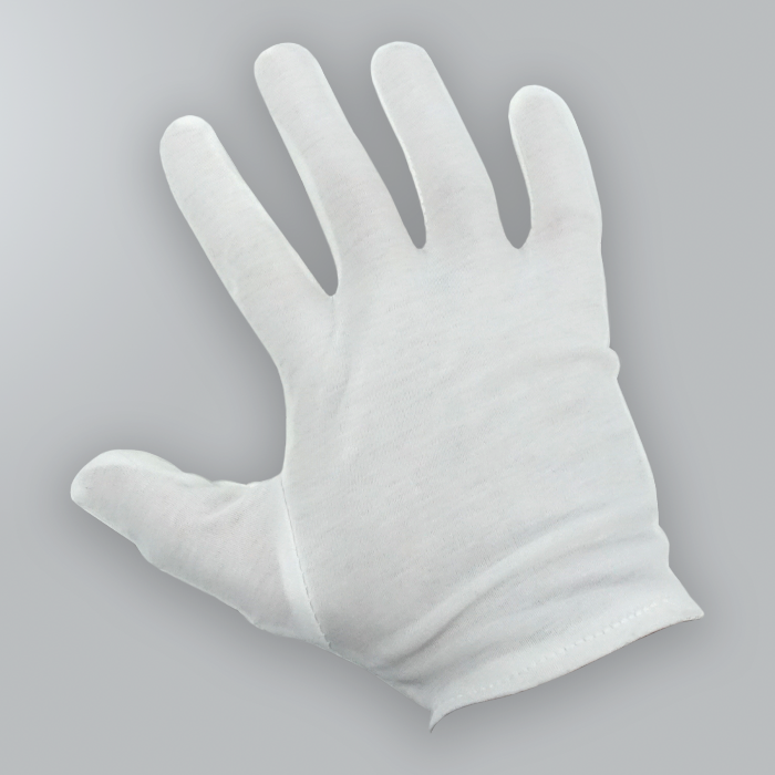
- Wear nitrile gloves when handling boards contaminated with capacitor electrolyte or corrosion.
- Dispose of waste solder, used flux and contaminated materials in accordance with WEEE 2013.
- Maintain a COSHH assessment for all chemical substances used in the workshop.
- Wash hands thoroughly after handling PCBs, particularly if lead-based solder is present.
3.Test Equipment
Having the correct test equipment, and knowing how to use it properly, is fundamental to efficient ECB diagnosis. The table below summarises the key tools, their primary uses, and important limitations.
| Instrument | Primary uses | Key limitations |
|---|---|---|
| Digital Multimeter (DMM) | DC/AC voltage; resistance; continuity; diode test; capacitance (some models) | Not suitable for signals above a few kHz; input impedance loads high-impedance nodes |
| Oscilloscope | Signal waveforms; timing; noise; PWM; clock integrity; rise/fall times | Probe ground lead introduces loop area, keep leads short; high-bandwidth probes required for fast signals |
| LCR Meter | Capacitor ESR & value; inductor value; component screening | In-circuit readings may be affected by parallel components — desolder one end before condemning a part |
| Logic Analyser | Multi-channel digital capture; protocol decode (I²C, SPI, UART, parallel bus) | Sampling rate must exceed 4–10× signal frequency for reliable capture |
| Thermal Camera / IR Thermometer | Detecting hot spots under power, overloaded regulators, shorted components, dry joints | Thermal camera gives best spatial resolution; IR thermometer is point-measurement only |
| Variable Bench PSU | Controlled power-up; current-limiting to protect board; voltage margining | Always set current limit before applying power to a suspect board |
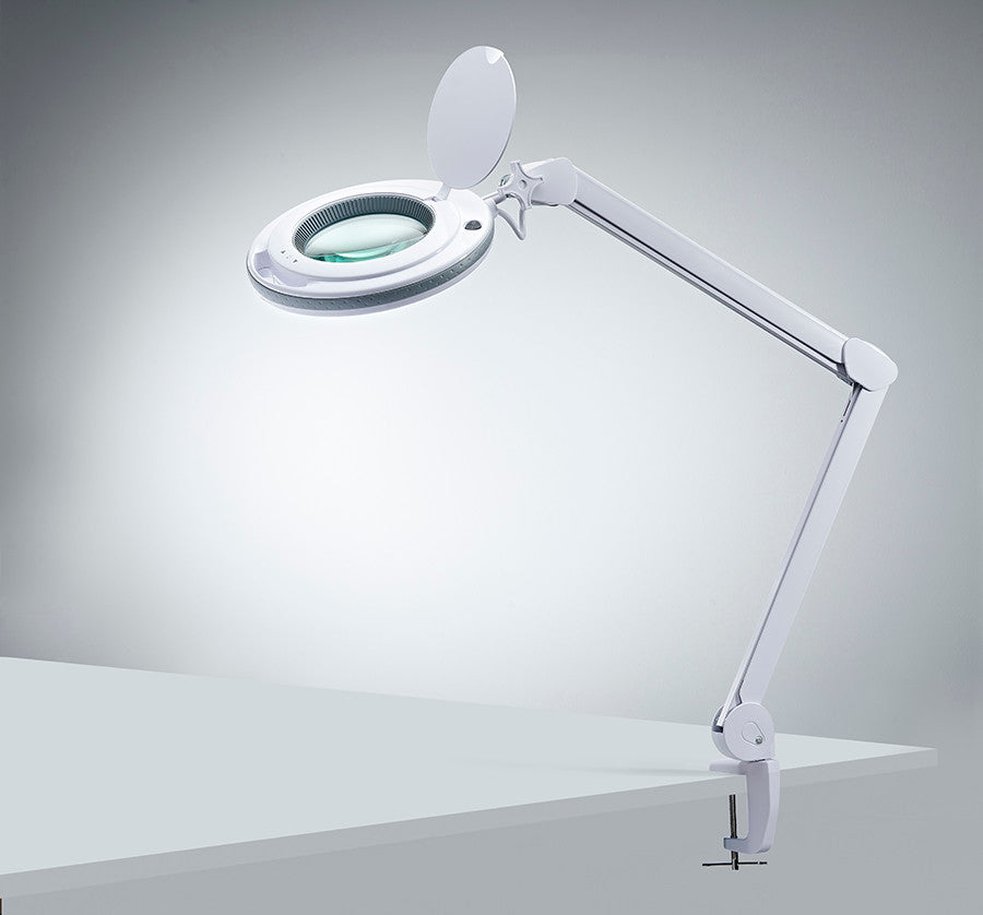
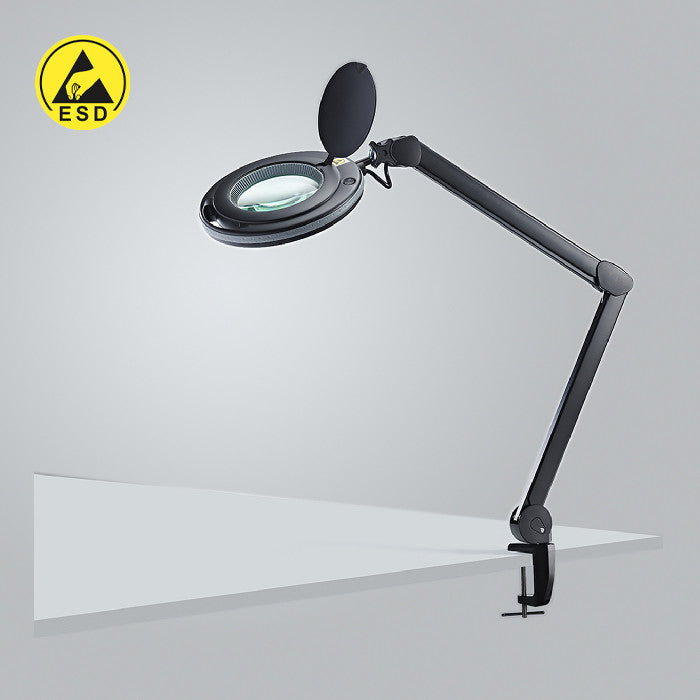
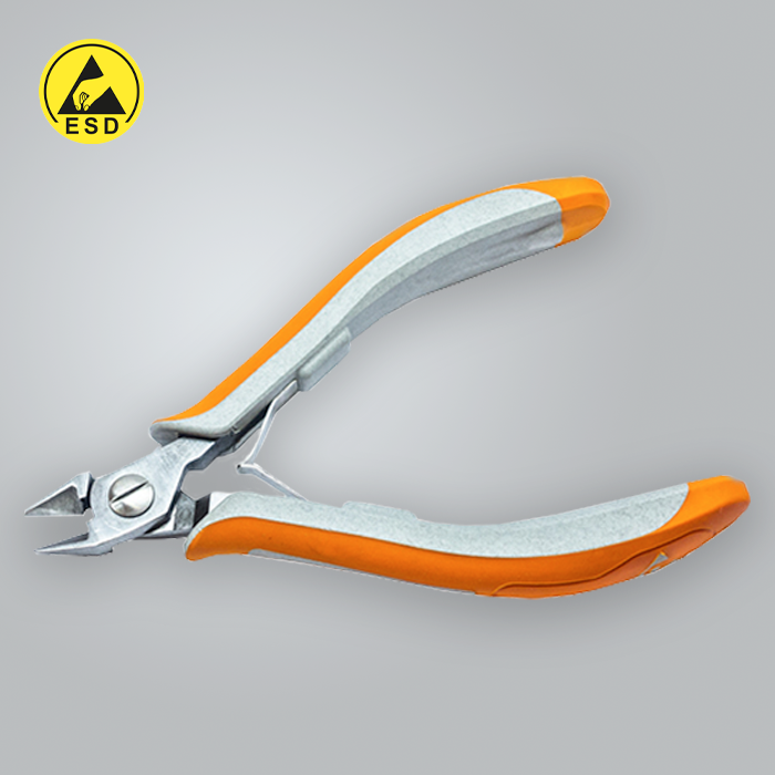
| Magnification (loupe / stereo microscope) | Inspection of fine-pitch solder joints, hairline cracks, SMD markings | Stereo microscope preferred for rework; 10–40× magnification sufficient for most inspection |

4.Systematic Fault Finding Process
Successful ECB fault finding depends on following a logical, structured process rather than replacing components at random. The recommended decision sequence is:
- Visual inspection — check for burns, damage, corrosion. If damage is visible, document and replace/repair.
- Check power supply — measure input voltage at the board. If the voltage is wrong, the fault is in the PSU or supply wiring.
- Component-level testing — measure resistance, continuity, capacitance. Replace any clearly-faulty component.
- Signal / logic testing — use an oscilloscope or logic analyser to verify clock, reset, and data signals.
- Repair, test and document — verify the fault is resolved, exercise all functions, and record findings.
Each stage is explained in detail in the sections that follow.