
Technical Guide • Part 2 of 2

Electronic Circuit Board — Repair & Rework Guide

A practical, step-by-step repair reference for electronics technicians, engineers, and advanced hobbyists. Written for a UK audience with reference to applicable international standards.

UK Edition v1.0 • April 2026

1.Introduction

Once a fault has been identified on an Electronic Circuit Board (ECB) using systematic diagnostic techniques, the next stage is competent, controlled repair. ECB repair demands patience, the correct tools, sound technique, and a thorough understanding of the materials involved. Poor rework can cause additional damage, introduce new faults, or compromise the long-term reliability of the repaired assembly.

This guide covers the full range of ECB repair and rework techniques applicable to both through-hole and surface-mount (SMD) assemblies, including soldering, desoldering, component replacement, track and pad repair, via repair, and the application and removal of conformal coatings. The procedures are consistent with IPC-7711/7721 (Rework, Modification and Repair of Electronic Assemblies), the internationally recognised standard for ECB repair.

2.Safety & Regulatory Requirements

2.1Regulatory Framework (UK)

All ECB repair and rework carried out in a UK professional or commercial environment is subject to:

  • Health and Safety at Work etc. Act 1974 (HSWA) — the primary duty on employers and employees to ensure safe working practices.
  • Electricity at Work Regulations 1989 (EAWRs) — all soldering and component work must be carried out with the board de-energised.
  • COSHH 2002 — governs solder, flux, solvents, IPA and conformal coatings; a written COSHH assessment must be in place for all substances used.
  • PUWER 1998 — governs the suitability and safe use of soldering stations, hot air rework tools and ancillary equipment.
  • WEEE Regulations 2013 — governs disposal of removed components, waste solder and contaminated materials.

2.2ESD Precautions

All ECB repair work must be carried out under full ESD precautions as specified in BS EN 61340-5-1 (UK/EU) or ANSI/ESD S20.20 (international):

  • Wear a tested and calibrated ESD wrist strap connected to a common bonding point throughout all handling and rework.
  • Work on a grounded ESD mat connected to the same common bonding point.
  • Store removed components in ESD-safe packaging immediately.
  • Take replacement components from ESD-safe packaging and handle them without touching leads or pins directly.

2.3Ventilation & Fume Extraction

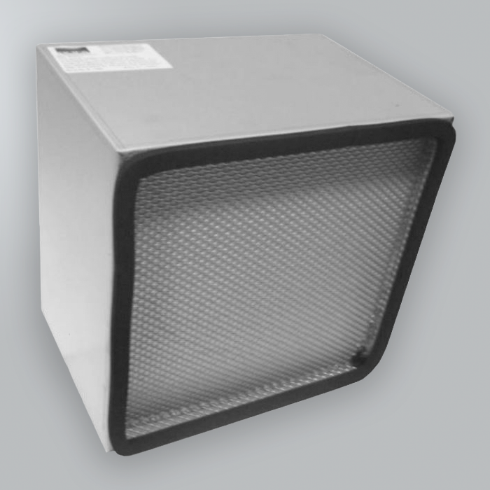
  • A fume extraction unit with a correctly rated filter must be positioned within 150 mm of the soldering point.
  • Filters must be replaced in accordance with the manufacturer's schedule and the COSHH assessment.
  • Lead-free solder fume is not harmless: SAC305 alloys produce tin and silver particulate which are respiratory hazards.
  • Lead-based solder (Sn63/Pb37) presents both fume and surface-contamination hazards: wash hands thoroughly and do not eat, drink or touch your face during or after soldering without washing first.

3.Tools, Materials & Workspace

3.1Essential Equipment

The following equipment is required for competent ECB repair work. Improvised or unsuitable tools are a leading cause of repair-induced damage and must not be used.

EquipmentSpecificationNotes
Soldering stationTemperature-controlled, 48–80 W, 200–480 °CNever use an uncontrolled mains iron on PCBs
Hot air rework stationAdjustable temperature and airflow; interchangeable nozzlesEssential for SMD removal; match nozzle to package size
SolderSAC305 (lead-free) or Sn63/Pb37 (leaded), 0.5–1.0 mm flux-coredMatch alloy to the original assembly where possible
FluxNo-clean or RMA rosin flux, pen or liquidWater-soluble flux must be fully cleaned after use
Desoldering toolsSolder sucker and desoldering braid (1.5–3.5 mm)Pre-flux the wick before use for better absorption
ESD tweezersFine-tip, anti-static, stainless steelKeep tips clean and undamaged
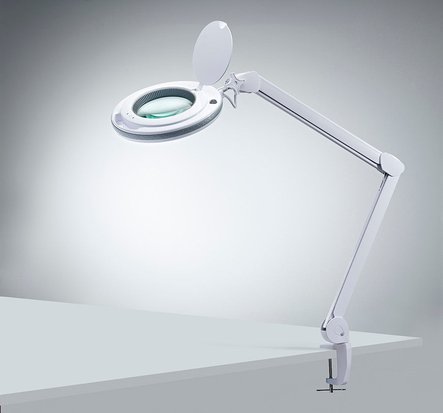
MagnificationStereo microscope (10–40×) or illuminated loupe (10× min.)Stereo microscope essential for fine-pitch SMD work
Cleaning materialsIPA 99%, ESD-safe brushes, lint-free swabsDo not use household cleaning products on PCBs
PCB holder / third handAdjustable, ESD-safe PCB vice or holderFree hands are essential for precise rework
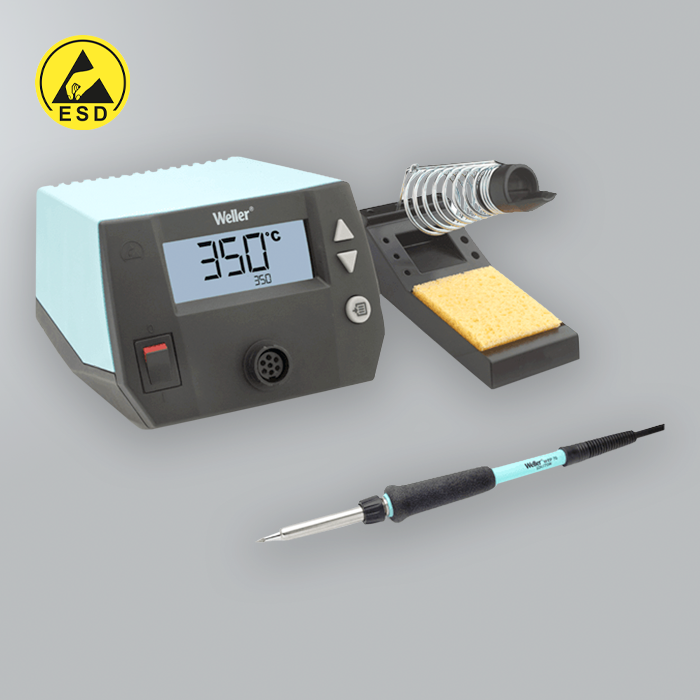
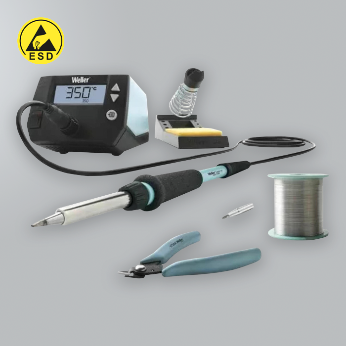
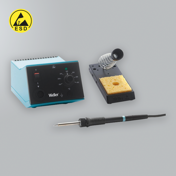
Essential soldering and rework equipment — temperature-controlled iron, solder and flux, desoldering and rework tools
Essential soldering and rework equipment.

3.2Soldering Iron Tip Selection & Maintenance

The iron tip is the most critical variable in soldering quality. An incorrectly selected, worn or poorly maintained tip causes the majority of rework defects.

  • Chisel tips (2–4 mm) — most versatile; through-hole joints, drag soldering, general SMD work.
  • Conical / pencil tips (0.5–1 mm) — fine-pitch SMD, targeted heat application.
  • Knife / hoof tips — drag soldering of fine-pitch QFP and SOIC packages.
  • Maintenance — tin the tip with fresh solder before and after each use; clean on a damp sponge or brass wool between joints; replace when the plating is visibly pitted, black or porous.

3.3Workspace Setup

  • Set up on a clean, clear ESD mat connected to a common bonding point.
  • Position the fume extraction unit within 150 mm of the work area.
  • Ensure adequate lighting and magnification appropriate to the component pitch.
  • Have all tools and materials within reach before starting, to minimise movement of the PCB.
  • Secure the PCB in a holder or vice — never solder a board resting loose on the bench.
  • Keep a lint-free cloth and IPA to hand for immediate tip cleaning and flux removal.

4.Soldering Techniques

4.1Principles of a Good Solder Joint

A solder joint functions both as a mechanical connection and an electrical conductor. Its quality depends on achieving proper wetting of both the component lead and the PCB pad, using the correct amount of solder, and allowing the joint to cool undisturbed. The internationally recognised acceptance criteria for solder joints are defined in IPC-A-610 (Acceptability of Electronic Assemblies). A good joint is bright and smooth with a concave fillet drawn toward the lead; a cold or dry joint is dull and grainy.

Solder joint quality reference — acceptable and unacceptable joint types
Solder joint quality reference (per IPC-A-610).

4.2The Soldering Process

Follow this procedure for every solder joint, whether through-hole or SMD:

  1. Ensure the iron tip is clean and fully tinned with fresh solder.
  2. Place the tip so it contacts both the component lead and the PCB pad simultaneously.
  3. Allow 1–2 seconds for the tip to heat both surfaces to soldering temperature.
  4. Apply solder to the joint (not the iron tip) and let it flow around the lead and wet the pad.
  5. Remove the solder first, then the iron tip.
  6. Allow the joint to cool completely without moving the component (typically 2–3 seconds).
  7. Inspect under magnification before moving to the next joint.

4.3Through-Hole Soldering

  • Apply the iron tip to the junction of the lead and the pad ring on the top (component) side of the board.
  • Feed solder into the joint from the same side. For plated through-holes, solder should flow through the barrel and appear as a small fillet on the underside.
  • A good through-hole joint has a concave fillet on both the top and bottom of the board, with the lead visible protruding through the solder on top.
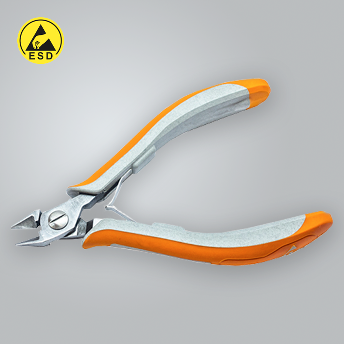
  • Trim leads to 1–1.5 mm above the solder fillet using flush cutters after soldering — trimming before risks disturbing the joint.
  • Typical parameters: iron at 340–370 °C, dwell time 3–4 seconds.

4.4SMD Soldering

Small passives (0402, 0603, 0805, MELF)

  1. Apply a small amount of flux to both pads.
  2. Tin one pad with a small amount of solder.
  3. Using tweezers, place the component on the pads and hold in position.
  4. Reflow the pre-tinned pad with the iron tip, allowing the component to settle into the solder.
  5. Release the tweezers once the solder has solidified.
  6. Solder the opposite pad with fresh solder, then inspect both joints and reflow the first if required.

SOIC / SOT packages

  • Align pin 1 carefully against the pad pattern before soldering.
  • Tack two diagonally opposite corner pins to fix the IC in position.
  • Solder the remaining pins using a fine tip and fine solder (0.5–0.7 mm).
  • For drag soldering: apply flux liberally, lay a small solder bridge across a row of pins, and drag the iron along the row in one smooth motion. Remove bridges with desoldering braid.

QFP / LQFP / TQFP packages

  • Align the IC using a stereo microscope — pin 1 orientation is critical.
  • Tack all four corner pins before soldering the remaining pins.
  • Use a hoof or knife tip for drag soldering fine-pitch leads; apply flux generously to improve flow and reduce bridging.
  • Inspect every lead under magnification and remove all bridges with braid before proceeding.

5.Desoldering & Component Removal

5.1Through-Hole Component Removal

Using a solder sucker

  1. Apply flux to the joint on the solder side of the PCB.
  2. Heat the joint with the iron until the solder is fully liquid.
  3. Immediately place the charged solder sucker nozzle over the joint and trigger.
  4. Remove the iron and inspect the hole; repeat if solder remains.
  5. Once all joints are clear, check the lead moves freely in the hole before extracting.

Using desoldering braid (wick)

  1. Apply flux to the braid before use to improve absorption.
  2. Lay the braid flat over the joint.
  3. Press the iron onto the braid and hold until solder is visibly absorbed.
  4. Lift the iron and braid together — never tear the braid from the joint while cold.
  5. Cut away the used (solder-saturated) section and repeat as necessary.
Through-hole component removal and replacement — four-step process
Through-hole component removal and replacement.

5.2SMD Component Removal

Small passives (2-terminal SMD)

  1. Apply flux to both ends of the component.
  2. Apply a little solder to one iron tip and touch both pads of the component simultaneously.
  3. Once both joints are liquid, lift the component away with tweezers.
  4. Alternatively, use hot air tweezers or a small hot air nozzle at 320–360 °C.

Multi-pin SMD (SOIC, SOT23, etc.)

  1. Apply flux to all leads.
  2. Set the hot air station to 340–380 °C, airflow medium (3–5).
  3. Hold the nozzle 5–10 mm above the component, moving in a slow circular motion.
  4. When all joints are liquid (typically 15–30 seconds), lift the component straight up with tweezers — do not tilt or rotate.

QFP / BGA and complex ICs

  • Select a nozzle that encompasses all four sides of the IC simultaneously.
  • Pre-heat the board underside with a preheater (100–150 °C) if available, to reduce thermal stress.
  • Apply hot air at 360–400 °C in a slow circular pattern; lift the IC with a vacuum pick-up or tweezers when all leads are liquid (30–60 seconds).
  • BGA rework requires a rework station with vision alignment — do not attempt it without appropriate training and equipment.
SMD component removal and replacement techniques for passives, SOIC/SOT and QFP packages
SMD component removal and replacement techniques.

6.PCB Track, Pad & Via Repair

Damaged tracks, lifted pads and failed vias can be repaired using the techniques defined in IPC-7711/7721. Work under magnification and address the root cause of any damage before repairing.

PCB track, pad and via repair techniques — wire bridge, lifted pad, via repair and conformal coating
PCB track, pad and via repair techniques.

6.1Broken Track Repair

  1. Using a scalpel or fine abrasive, expose clean copper at both ends of the break, removing solder resist and oxidation.
  2. Apply flux to both exposed areas and tin them lightly.
  3. Cut a short length of fine copper wire (28–32 AWG) to bridge the gap.
  4. Solder one end of the wire to each tinned area, ensuring it lies flat against the board.
  5. Inspect the repair under magnification for good wetting and continuity.
  6. Cover the repair with insulating varnish or conformal coating.

6.2Lifted Pad Repair

  • If only partially lifted, clean the underside and re-adhere with a small amount of non-conductive PCB adhesive (epoxy), allowing it to cure fully before soldering.
  • If completely detached or severely damaged, route a jumper wire from the component lead to the nearest accessible point on the track, or to a via on the same net.
  • Anchor the jumper wire with adhesive before soldering to prevent movement.
  • Inspect the original track for damage beyond the pad area and repair as required.

6.3Via Repair

Failed vias — typically caused by cracked barrel plating from thermal cycling — are among the most difficult intermittent faults to repair reliably.

Solder-fill method

  1. Clean the via and surrounding area with IPA.
  2. Apply flux to the via barrel from both top and bottom.
  3. Apply solder from the top, heating from the bottom until it flows through the barrel.
  4. Inspect from both sides for full fill and good wetting of the pad rings.

Jumper-wire method: thread a fine wire through the via, solder to the pad ring on each side, and trim flush. Eyelet / rivet method: a swaged copper eyelet (0.3–1.5 mm) forms a new barrel conductor — the most robust repair where the via sees repeated thermal cycling.

6.4Conformal Coating Removal & Reapplication

Removal: solvent (IPA / specialist remover) for no-clean and acrylic coatings; scoring and peeling for silicone; careful micro-abrasion for hard polyurethane.

Reapplication

  1. Clean the repaired area with IPA and allow to dry completely.
  2. Mask adjacent areas that must not be coated (connectors, test points, heatsink contacts).
  3. Apply coating by brush for small areas or aerosol for larger — two thin coats are preferable to one thick coat.
  4. Allow to cure per the manufacturer's specification before powering the board.